Micro/Nano Fabrication Facility
Georgia Institute of Technology
Contact: Billyde Brown
Phone: (404)-894-0479
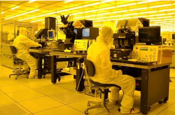
These facilities comprise hands-on, shared user cleanroom space the Marcus and Pettit buildings. These cleanrooms are general use for electronics, MEMS, photonics, and materials research, along with specialized labs for work at the interface between fabrication and life sciences and a laser machining lab for micro-machining of diverse materials.
All of the more than 200 individual tools, with substrate capabilities up to 150mm, are accessible to both internal and external clients for hands-on use. Training requests, scheduling, and routine communications are all handled through a web-based interface, and in-the- lab access is controlled with an electronic access control system which documents all usage for subsequent billing and statistical analysis.
The major tool categories are:
- Lithography/Patterning: UV Photolithography (365nm, 405nm, 248nm), Nano-imprint, E-beam Lithography, Laser (Maskless) Lithography, Inkjet Printing, Soft Lithography
- Dry Etching: Silicon/Polysilicon DRIE, Silicon/Polysilicon RIE, Silicon Dioxide (quartz, fused silica) DRIE, Silicon Nitride DRIE, III-V Semiconductor DRIE, RIE, Metal RIE
- Wet Etching: Semiconductors, Dielectrics, Metals, Organic Materials
- High Temperature Processes: Oxidation, Annealing, Polymer Curing, Diffusion Doping, Drive-in, Sintering, Rapid Thermal Processing
- Thin Film Deposition: RF/DC Sputtering, Co-sputtering, Evaporation, ALD, PECVD, APCVD, LPCVD
- Polymer Deposition: Spin Coating, Spray Coating, CVD (Parylene)
- Plating: Electroplating & Electroless Plating
- Packaging: Wire bonding, Wafer bonding, Anodic bonding, Thermal compression bonding, Eutectic bonding, Flip-Chip bonding, Chemical Mechanical Polishing, Lapping, Lamination
Visit the website of the Micro/Nano Fabrication Facility »
< Back to GRA Core Exchange facilities

